Semiconductor Research and Fabrication Facility Celebrates Topping Out

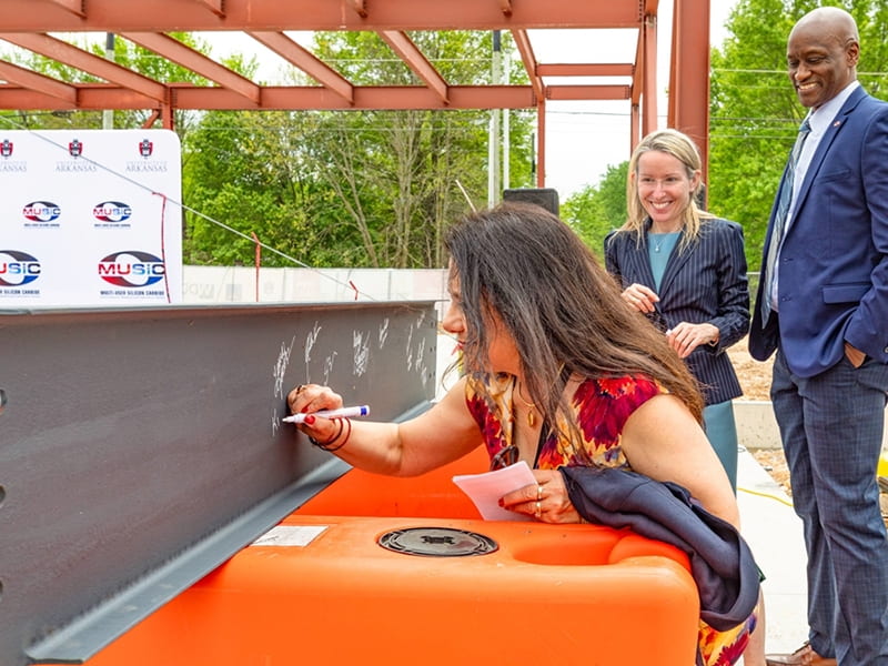
From left, Kim Needy, dean of the College of Engineering, signs a beam while Margaret Sova McCabe, vice chancellor for research and innovation, and Chancellor Charles Robinson observe.
The U of A celebrated a milestone with the topping-out of the Multi-User Silicon Carbide Research and Fabrication Facility.
More than 100 students, faculty, state leaders and citizens were on hand to sign the steel topping-out beam and hear remarks from Kim Needy, dean of the College of Engineering, and Alan Mantooth, Distinguished Professor of electrical engineering.
The new semiconductor research and fabrication facility will produce microelectronic chips made with silicon carbide, a powerful semiconductor that outperforms basic silicon in several critical ways. The facility will enable the federal government – via national laboratories – businesses of all sizes and other universities to prototype with silicon carbide, a capability that does not presently exist elsewhere in the United States.
Work at the research and fabrication facility will bridge the gap between traditional university research and the needs of private industry and will accelerate technological advancement by providing a single location where chips can go from developmental research to prototyping, testing and fabrication.
The 21,760-square-foot facility, located next to the National Center for Reliable Electrical Power Transmission at the Arkansas Research and Technology Park, will address obstacles to U.S. competitiveness in the development of silicon-carbide electronics used in a wide range of electronic devices, circuits and other consumer applications. The building will feature approximately 8,000 square feet of clean rooms for fabrication and testing.
Education and training within the facility will also accelerate workforce development, helping supply the next generation of engineers and technicians in semiconductor manufacturing.


